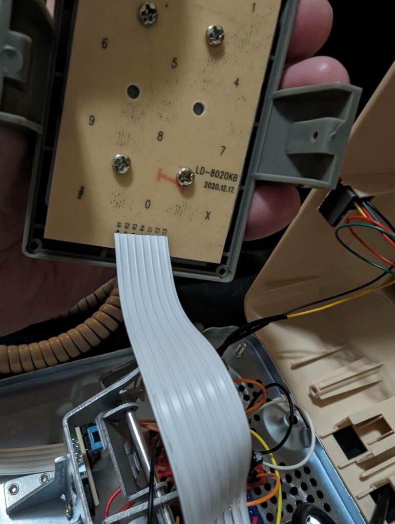
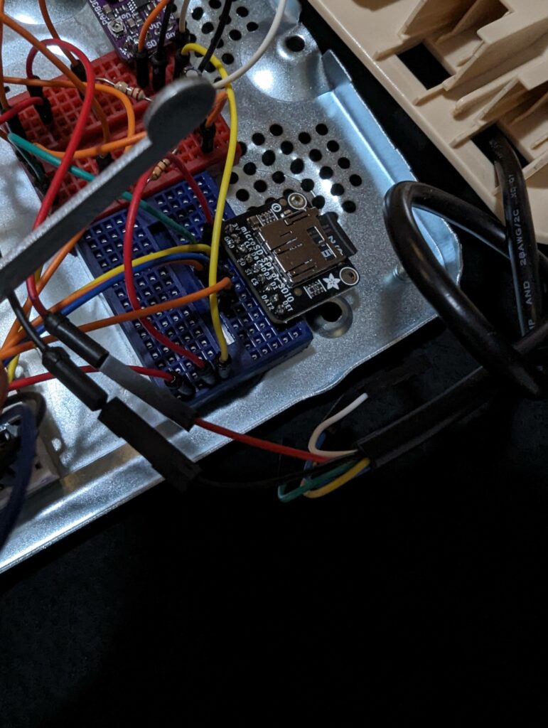
Next up we’re going to take that phone apart! But first, remember to refer to the source!
https://learn.adafruit.com/touch-tone-phone-dial-a-song/build-the-dial-a-song-circuit
So it shows the circuit a few different ways. There’s an illustration of the circuit on a breadboard. (is it right? I’m not sure!) There’s a diagram! (Is that right? Some is, but some is definitely broken!) Then there’s a bunch of pictures. (How about those? They’re what I used, so yes?)
The first set of photos are for the amplifier. You should have already soldered a set of 5 pins to this, and two pins for the audio out connector. The 5 pins are (left to right) A+, A-, SD, Vin, Gnd. A- and Gnd need to get to a common ground. Vin connects to a 3 volt source. And SD doesn’t need to connect to anything. A+ connects via a series of two resistors to the TX connector on the Feather. Between the two resistors place the capacitor, and connect it to ground. Note the capacitor has a positive and negative side. Negative side goes to ground.
Next is the keypad. The instructions have a lot of desoldering and adding pins, etc. None of that is necessary.


Looking at the second photo first, you can see the rows and columns of the keypad next to the cable (while they are labeled in this case, they may not be. See upcoming “Troubleshooting” page for help if they aren’t). If you look at the first photo, you can see the end of the cable popping up behind the keypad with a bunch of jumpers going into it.
Also, as you can see in the phone here, I have removed everything except for the connector for the handset, the connector and switch for the disconnect hook, and the keypad. You can get rid of everything else. You’re going to need that space for the little self-adhesive breadboards.
Anyway, one nice thing about not doing it the way they say to, is it doesn’t lock you into using the pins on the Feather that the instructions recommend. And one of the reasons that we want to avoid that is that the SD card interface likes to use some of the pins that the instructions use for the keypad. To summarize:
| Keypad Columns/Rows | Instructions | My Circuit |
| C1 | A3 | A3 |
| C2 | A2 | A2 |
| C3 | A1 | A1 |
| R1 | D24 | D24 |
| R2 | D25 | D25 |
| R3 | SCK | D4 |
| R4 | MOSI | D5 |
Since we’re here, lets also talk about the SD card reader.

Once you solder the pins onto the board, you may be confused, since there are a LOT of pins. You only need the first six. 3V, Gnd, Clk, SO, SI, and CS.
3V connects to the same 3 volt source you’re using for the amplifier. That also connects to the 3V pin on the Feather. Gnd connects to the same ground you’re using for the amplifier. Again, this also connects to the Gnd pin on the Feather.
CLK connects to the SCK pin on the Feather. SO connects to the Feather’s MI pin. SI connects to the MO pin. (Remember MISO and MOSI). Finally, the CS pin needs to connect to a data pin on the Feather. I used D10.
Side note: Some of the pins on the Feather use the same data addresses. My understanding is that this could theoretically cause issues if you have two pins with the same address trying to operate at the same time. I chose all the pins so that they wouldn’t conflict with any other pins.
Next up, More Phone Guts?
2 thoughts on “Phone-Modding Part 3 – Circuitry and Phone Guts”